Spectroscopy 2.0 is a fresh breakthrough that transforms how we study and understand materials at their deepest level. It blends cutting-edge techniques that stretch the limits of both time and space. As a result, we can now observe phenomena that once felt completely out of reach for scientists.
The Three Methodologies Behind Spectroscopy 2.0:
At the heart of Spectroscopy 2.0 sit three game-changing techniques that push scientific discovery forward.
- Femtosecond science captures reactions unfolding in just quadrillionths of a second. It freezes ultra-fast events, so researchers can finally see what was once invisible.
- Raman mapping steps in with incredible spatial detail. It shows how chemical compositions shift across a surface, revealing patterns and hidden variations.
- XPS surface analysis adds another layer of insight. It reads the topmost atomic layers of a material. This process delivers precise elemental information. It helps us understand how surfaces behave and why they matter.
Together, or even used on their own, these methods unlock details that older spectroscopy approaches simply couldn’t reach. They open the door to clearer, deeper, and more reliable scientific answers.
The Impact of Spectroscopy 2.0
The significance of these advancements spans various scientific fields:
- Chemical reactions can now be observed as they happen.
- Material heterogeneities can be mapped at the nanoscale level.
- Surface chemistry can be characterized with unparalleled precision.
This new ability could completely change the game for researchers working in:
- Designing novel materials
- Understanding catalytic processes
- Advancing nanotechnology applications
Femtosecond Spectroscopy: Probing Ultrafast Dynamics
Femtosecond spectroscopy works on timescales that are almost impossible to imagine, one femtosecond is 10^-15 seconds, or a millionth of a billionth of a second. To grasp this, think of it this way: a femtosecond compared to a second is like a second compared to 32 million years. This mind-boggling speed lets scientists watch the fastest fundamental processes in matter, events that were completely hidden before.
The Principle Behind Femtosecond Science
Femtosecond spectroscopy is built on creating and controlling ultrafast laser pulses. These pulses serve a dual purpose: they trigger a process in a material and then probe its changes in real time. The method usually uses a pump-probe setup. First, a pump pulse excites the sample, pushing it into a non-equilibrium state. Then, probe pulses examine the system at carefully timed intervals.
Generating such ultrashort pulses requires advanced mode-locking techniques in lasers. Ti:sapphire lasers are the main workhorse in femtosecond spectroscopy. They produce pulses lasting from just a few femtoseconds up to hundreds of femtoseconds. The shorter the pulse, the higher the temporal resolution, letting us capture faster dynamics more clearly.
Capturing Molecular Motion in Real Time
When femtosecond pulses hit a material, you can actually watch molecules move. Electrons jump between energy levels in just 1–100 femtoseconds. Traditional spectroscopy could only guess these jumps from steady-state measurements. Femtosecond spectroscopy, however, captures them in real time.
Molecular vibrations are another fascinating area. Chemical bonds stretch, bend, and twist over tens to hundreds of femtoseconds. With femtosecond techniques, we can follow these vibrations directly and see how energy flows through a molecule after it absorbs light. This opens doors to understanding:
- How energy transfers in photosynthesis
- How charges separate in solar cells
Moreover, Raman spectroscopy often works alongside femtosecond methods. Together, they provide extra insights into molecular vibrations and other fast dynamic processes.

Raman Mapping Techniques: Spatially Resolved Chemical Imaging
Raman spectroscopy is a powerful tool for exploring materials at the molecular level. It works by shining a special light on a sample and studying the light that bounces back. Most of the light reflects unchanged, but a tiny fraction interacts with the molecules, making them vibrate. This causes a small shift in the light’s energy, which we can measure to identify chemical structures and compounds.
One big advantage of Raman spectroscopy is that it needs little to no sample preparation. You can study solids, liquids, or gases in their natural state. The vibrations recorded in a Raman spectrum match specific functional groups and atomic arrangements. This makes Raman spectroscopy perfect for identifying unknown substances and tracking chemical reactions in real time.
Unlock deeper molecular insights with the book Raman Spectroscopy for Chemical Analysis — your ultimate guide to mastering modern analytical chemistry.
From Point Analysis to Spatial Mapping
Raman mapping transforms the old method of analyzing a single point into a powerful way to study whole surfaces. Instead of focusing on just one spot, the laser scans across the sample, collecting spectra from many points. This produces a detailed map that reveals how molecules are spread across the material.
When performing Raman mapping, you can adjust several key parameters to get the best results:
- Step size: This sets how close each measurement point is. Smaller step sizes capture finer details and boost spatial resolution.
- Scan area: This defines the region you’ll analyze. You can focus on specific features or explore larger sections of your sample depending on your goals.
- Integration time: This balances signal quality and speed. Longer integration times give clearer signals but slow down data collection.
- Laser wavelength: Different materials respond differently to various wavelengths. Choosing the right wavelength for your sample improves sensitivity to specific molecular vibrations.
Modern confocal Raman systems also let you create three-dimensional images. By adjusting the laser focus depth, you can explore internal structures without cutting or damaging the sample.
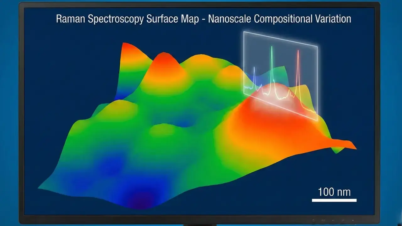
Revealing Material Heterogeneities at the Nanoscale
Raman mapping is a powerful tool for revealing subtle differences in composition and structure that bulk analysis methods often miss. Advanced systems in this technique can reach spatial resolutions of about 200–300 nanometers, right at the diffraction limit. This lets us see nanoscale features that strongly influence how materials behave.
By collecting and combining Raman spectra from various regions within a single sample, we can uncover detailed insights into…
XPS Surface Analysis: Elemental and Chemical State Characterization at the Surface
X-ray photoelectron spectroscopy, also called Electron Spectroscopy for Chemical Analysis (ESCA), is a top-notch surface analysis tool in modern spectroscopy. It gives precise, quantitative insights into the elements and their chemical states on the very surface of materials. This makes it indispensable for exploring surface chemistry at the nanoscale.
The Photoelectric Effect in Action
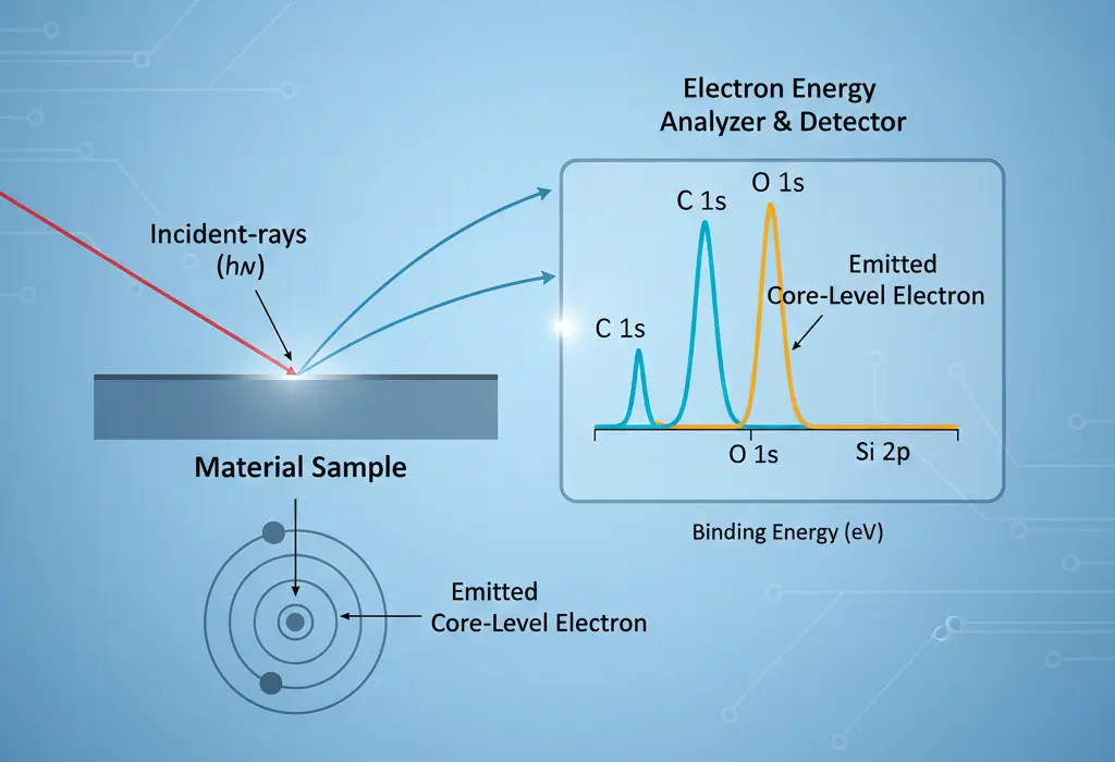
XPS works on the principle of the photoelectric effect. When X-rays hit a material’s surface, their high-energy photons interact with atoms. This energy transfers to core electrons. If the X-ray energy is higher than the electron’s binding energy, the electron escapes and moves toward the surface.
These emitted electrons, called photoelectrons, have specific kinetic energies that we can measure precisely. The electron’s original binding energy is found using this formula:
Binding Energy = X-ray Energy − Kinetic Energy − Work Function
Every element has unique binding energies, forming a distinct spectroscopic fingerprint. By studying these energy patterns, we can identify all elements on the sample surface—except hydrogen and helium. The height of each peak shows how much of that element is present.
👉 Want to dive deeper into XPS and AES? Check out An Introduction to Surface Analysis by XPS and AES — a must-read for anyone exploring modern surface chemistry.
Chemical State Sensitivity: Beyond Simple Elemental Analysis
XPS surface analysis is great for spotting different chemical states of the same element. When an atom forms chemical bonds, the electron cloud around its nucleus changes. This causes small shifts in binding energies, usually between 1–5 eV. These “chemical shifts” help us tell apart oxidation states, molecular environments, and bonding types.
For example, XPS can easily distinguish metallic iron from iron oxide. It can also identify carbon as graphite, carbonate, or part of an organic molecule. This information is especially important for studying catalysts, because the oxidation state of metal centers directly affects how well they function.
Extreme Surface Sensitivity
The standout feature of XPS is its incredible surface sensitivity. Photoelectrons generated deep inside a material scatter many times before reaching the surface. This means only electrons from the top few nanometers actually contribute to the XPS signal.
Because of this, XPS is perfect for studying surfaces and interfaces. Whether it’s thin films, coatings, or nanoparticles, XPS reveals their composition and chemical states—details that bulk analysis methods simply can’t capture.
In short, XPS combines elemental analysis with chemical state detection right at the surface. Its ability to probe nanoscale layers opens exciting possibilities in materials science, catalysis, semiconductors, and beyond.
Integration of Femtosecond Spectroscopy, Raman Mapping & XPS Analysis in Modern Research
The Power of Spectroscopy 2.0: Modern femtosecond science truly shines when we combine advanced techniques. By integrating different spectroscopy methods, we can explore materials in ways single techniques can’t. This approach lets us see changes across time, space, and chemical structure, all at once, giving a richer, more complete picture.
Real-Time Structural Monitoring Through Combined Femtosecond-Raman Analysis
Pairing femtosecond spectroscopy with Raman mapping lets us watch structural changes unfold in both time and space. Femtosecond laser pulses trigger ultrafast processes in the material. Meanwhile, Raman mapping tracks molecular vibrations and structural shifts at specific spots. Together, they reveal how energy moves through the material, where defects appear, and how different regions respond to stimulation.
This approach makes it possible to observe photocatalytic reactions in real time. You can follow the formation of intermediate species with femtosecond precision while at the same time mapping their location across catalyst surfaces. The femtosecond pulses capture the initial electronic excitations and charge transfers within picoseconds. At the same time, Raman mapping shows which molecular bonds break or form and exactly where these changes happen in your sample.
The Complementary Power of XPS in Multimodal Characterization
Multimodal characterization takes a big leap when you add XPS surface analysis to your femtosecond-Raman setup. Femtosecond spectroscopy shows when processes happen, and Raman mapping shows where they occur. XPS adds the missing piece: it tells you what chemical species are present and their exact oxidation states. Together, this three-dimensional view, time, space, and chemistry, offers deep insight into material behavior.
Start by using XPS to check the initial surface chemistry. Then, apply femtosecond-Raman methods to track dynamic processes in real time. Finally, return to XPS for post-reaction analysis. This before-during-after workflow uncovers not only reaction kinetics but also the lasting chemical changes caused by ultrafast phenomena.

Applications Across Scientific Fields Using Spectroscopy 2.0
Femtosecond spectroscopy, Raman mapping, and XPS analysis have completely changed how we study materials in research. Together, they provide the precision and speed needed to design materials with properties tailored for specific technologies.
Materials Science and Thin Film Engineering
These advanced spectroscopic methods let us explore thin film coatings like never before. XPS pinpoints the chemical composition and bonding in just the first few nanometers of a film. Meanwhile, Raman mapping shows how crystallinity and stress vary across the surface. Add femtosecond spectroscopy, and you can track carrier dynamics and charge transfer, key factors for electrical and optical performance.
Nanomaterial interfaces are especially tricky, but Spectroscopy 2.0 handles them well. At the junctions between materials, such as semiconductor heterostructures or metal-oxide interfaces, you need to assess the static chemical makeup. It is also important to understand the dynamic electronic behavior. XPS captures the elemental fingerprint at these boundaries. Femtosecond methods reveal electron transfers happening in quadrillionths of a second, giving a complete picture of what’s really going on.
Unlock deeper insights with Materials Science of Thin Films: Deposition and Structure — the essential book every researcher and student should explore.
Chemistry: Unraveling Reaction Mechanisms
Catalysis research gains a huge advantage from femtosecond spectroscopy, which captures reaction intermediates that exist for just a few femtoseconds. You can watch chemical bonds break and form in real time, uncovering reaction details that were once hidden. Pairing this timing information with Raman mapping shows exactly where reactions happen fastest on a catalyst surface, helping design more efficient catalytic materials.
Photochemical reactions show how powerful these techniques are. Femtosecond pulses trigger reactions and track how excited states evolve. Meanwhile, XPS analysis before and after light exposure confirms the chemical changes at the molecular level.
Physics: Electronic Structure at Ultrafast Scales
Physics research is constantly pushing the limits of time resolution to explore the tiniest electronic processes. It lets us see how electrons react to light, how energy spreads through vibrations in a material, and how quantum states change over time.
Future Perspectives & Challenges in Spectroscopy 2.0
The world of Spectroscopy 2.0, covering femtosecond science, Raman mapping, and XPS surface analysis, is evolving fast. Researchers are constantly discovering new ways to explore materials. Looking ahead, spectroscopy is likely to shift toward advanced techniques that blend multiple types of analysis for deeper insights.
Promising Directions in Nanoscale Imaging
One of the most exciting breakthroughs in nanoscale imaging is the rise of correlative spectroscopy-microscopy platforms. These systems combine the power of spectroscopy with electron or scanning probe microscopy, giving a fuller view of materials.
With these platforms, you can:
- Observe structural changes and chemical transformations in materials simultaneously.
- Understand material behavior better by linking surface features with chemical composition.
A great example is atomic force microscopy paired with Raman spectroscopy (AFM-Raman). This combination lets researchers explore both structure and chemistry at the nanoscale.
Revolutionizing Data Analysis with Machine Learning
Machine learning is changing the way we analyze spectroscopic data. Using deep learning, we can now:
- Spot subtle spectral patterns that humans might miss
- Automatically classify complex material phases
- Predict material properties from spectroscopic fingerprints
Neural networks trained on large spectral databases can turn hours of analysis into mere seconds. This is a huge benefit, especially when handling the massive datasets produced by Raman mapping experiments.
Challenges Ahead
Despite these promising developments, there are still significant challenges to overcome in the field of ultrafast analysis.
Balancing Temporal Resolution and Spatial Detail
One big challenge is balancing time and space. Shorter femtosecond pulses can capture events faster, but they often reduce photon flux. This drop makes the signal noisier.
To reach sub-10 femtosecond resolution while keeping sharp nanoscale details, we need smart approaches. Techniques like pulse compression and more sensitive detectors can help overcome this hurdle.
Overcoming Technical Barriers in Integration
Another challenge lies in integrating different techniques like femtosecond spectroscopy, Raman mapping, and XPS (X-ray Photoelectron Spectroscopy). This requires significant technical innovation to overcome issues such as:
- The incompatibility between ultra-high vacuum conditions needed for XPS measurements and atmospheric conditions typically used for Raman measurements
- Sample degradation during transitions between different analytical chambers
- Contamination risks when transferring samples between these chambers
Pushing Boundaries with Instrumentation Miniaturization
Miniaturizing instruments is opening a whole new frontier for spectroscopy.
Smaller, portable devices allow scientists to analyze samples on-site, wherever they are. They also make it possible to study materials that traditional setups can’t reach. This could unlock breakthroughs in understanding complex systems, like working catalysts or delicate biological samples.
Researchers are pushing the limits with hybrid methods, machine learning, and advanced instruments. We can expect exciting discoveries in material characterization soon!
Conclusion
Spectroscopy 2.0 is transforming the way we study materials at their core. Modern tools like femtosecond spectroscopy, Raman mapping, and XPS surface analysis make it possible to explore matter faster and more precisely than ever before. They let us gather nanoscale information in real time—something that was once impossible.
By combining these techniques, you can:
- Watch chemical reactions unfold in femtoseconds
- Explore surface variations with nanometer-level detail
- Decode surface chemistry through precise elemental and chemical data
- Link time and space for a full picture of materials
Science is entering a new era of collaboration. Materials scientists, chemists, physicists, and nanotechnologists are now speaking the same language. Insights from these techniques are driving progress in catalysis, energy materials, semiconductors, and biomedical research.
Innovation is key. We must push instrument limits, analyze data smarter, and integrate techniques seamlessly. Global challenges like sustainable energy and advanced computing demand the full power of these methods.
By mastering these tools, you can spark breakthroughs that redefine technology. You can also deepen our understanding of the very building blocks of matter. Do you think you master science? test you knowledge by taking our Physical Chemistry Quiz test.
Frequently Asked Questions about Spectroscopy 2.0
Spectroscopy 2.0 is the next level of spectroscopic techniques, including femtosecond spectroscopy, Raman mapping, and XPS surface analysis. These tools let scientists observe materials in real time, explore chemical compositions across tiny areas, and study surface chemistry in amazing detail. By offering ultrafast and nanoscale resolution, Spectroscopy 2.0 is driving major breakthroughs in materials science, chemistry, physics, and nanotechnology.
Femtosecond spectroscopy uses ultrafast laser pulses lasting just a few quadrillionths of a second (10^-15 s) to watch electronic changes, molecular vibrations, and chemical reactions in real time. By combining pulsed lasers with sensitive detectors, it captures events that happen too fast for traditional methods. Scientists use it to explore how electrons move, how reactions unfold, and how materials behave under fleeting conditions.
Raman mapping takes vibrational spectroscopy a step further by scanning surfaces to create detailed chemical images. This technique uncovers variations in materials and reveals tiny structural features, helping us understand complex composites and spot defects. To get high-resolution images, it relies on precise scanning tools and sensitive detectors, making it essential for advanced materials analysis.